Showing posts with label Electronics. Show all posts

Friday, May 18, 2012

Pseudo Random Sequence Generator in Verilog


Pseudo Random Sequence is widely used in spread spectrum communication, to spread and de-spread the information sequence. The following diagram shows a PN sequence generator which has 3 memory elements, leads to processing gain 7 (2^3 - 1). According to the diagram, if the initial state is all zero, then the sequence will also be all zeros which is not usable.


Behavioural Model

module PNSeqGen(
    input clk, reset,
    output s3
    );
reg s1, s2, s3;
wire s0;
// MODULO 2 ADDITION
assign s0 = s1 ^ s3;
// STATE MACHINE
always @ (posedge clk or reset) begin
// INITIAL STATE SHOULDN'T BE 000 => 100
if(reset) begin
s1 <= 1;
s2 <= 0;
s3 <= 0;
end else begin
s1 <= s0;
s2 <= s1;
s3 <= s2;
end
end
endmodule

Test Bench

`timescale 1ns / 1ps
module Test_PNSeqGen;
// Inputs
reg clk;
reg reset;
// Outputs
wire s3;
// Instantiate the Unit Under Test (UUT)
PNSeqGen uut (
.clk(clk), 
.reset(reset), 
.s3(s3)
);
initial begin
// Initialize Inputs
clk = 0;
reset = 0;
// Wait 100 ns for global reset to finish
#100;
// Add stimulus here
#10 reset = 1;
#10 reset = 0;
#200 $finish;
end
always begin
#5 clk = ~clk;
end
// PRINT SEQUENCE
always @ (posedge clk) $write("%b",s3);      
endmodule

Output

001110100111010011101

Tuesday, May 8, 2012

4 Bit Priority Encoder in Verilog


Priority Encoder is an encoder circuit that includes a priority function. The operation is such that if two or more inputs are equal to 1 at the same time, the input having the highest priority will take precedence. 
Here, the priority decreases from right to left in the input. D[3] has the highest priority. V indicate the validity of the input (atleast one input should be 1) and the Y gives the output.(01 means 1, 10 means 2 like that...)


Behavioural Model : 4 Bit Priority Encoder

module PriorityEncoder_4Bit(
    input [0:3] D,
    output [1:0] Y,
    output V
    );
reg [1:0] Y;
reg V;
always @(D)
begin
Y[1] <= D[2] | D[3];
Y[0] <= D[3] | D[1] & ~D[2];
V = D[0] | D[1] | D[2] | D[3];
end
endmodule

Test Bench : 4 Bit Priority Encoder

module PriorityEncoder_4Bit_Test;
// Inputs
reg [3:0] D;
// Outputs
wire [1:0] Y;
wire V;
// Instantiate the Unit Under Test (UUT)
PriorityEncoder_4Bit uut (
.D(D), 
.Y(Y), 
.V(V)
);
initial begin
// Initialize Inputs
D = 0;
// Wait 100 ns for global reset to finish
#100;        
// Add stimulus here
#10 D = 4'b0000;
#10 D = 4'b1000;
#10 D = 4'b0100;
#10 D = 4'b0010;
#10 D = 4'b0001;
#10 D = 4'b1010;
#10 D = 4'b1111;
end
initial begin
$monitor("time=",$time,, "D=%b : Y=%b V=%b",D,Y,V);
end      
endmodule

Simulation Results

time= 000, D=0000 : Y=00 V=0
time= 120, D=1000 : Y=00 V=1
time= 130, D=0100 : Y=01 V=1
time= 140, D=0010 : Y=10 V=1
time= 150, D=0001 : Y=11 V=1
time= 160, D=1010 : Y=10 V=1
time= 170, D=1111 : Y=11 V=1

Wednesday, February 29, 2012

4 Bit Carry Look Ahead Adder in Verilog


DataFlow Model : 4 Bit CLA

module CLA_4bit(
    output [3:0] S,
    output Cout,PG,GG,
    input [3:0] A,B,
    input Cin
    );
    wire [3:0] G,P,C;

    assign G = A & B; //Generate
    assign P = A ^ B; //Propagate
    assign C[0] = Cin;
    assign C[1] = G[0] | (P[0] & C[0]);
    assign C[2] = G[1] | (P[1] & G[0]) | (P[1] & P[0] & C[0]);
    assign C[3] = G[2] | (P[2] & G[1]) | (P[2] & P[1] & G[0]) |             (P[2] & P[1] & P[0] & C[0]);
    assign Cout = G[3] | (P[3] & G[2]) | (P[3] & P[2] & G[1]) | (P[3] & P[2] & P[1] & G[0]) |(P[3] & P[2] & P[1] & P[0] & C[0]);
    assign S = P ^ C;
    
    assign PG = P[3] & P[2] & P[1] & P[0];
    assign GG = G[3] | (P[3] & G[2]) | (P[3] & P[2] & G[1]) | (P[3] & P[2] & P[1] & G[0]);
endmodule

Test Bench : 4 Bit CLA

module Test_CLA_4bit;
    // Inputs
    reg [3:0] A;
    reg [3:0] B;
    reg Cin;

    // Outputs
    wire [3:0] S;
    wire Cout;
    wire PG;
    wire GG;

    // Instantiate the Unit Under Test (UUT)
    CLA_4bit uut (
    .S(S), 
    .Cout(Cout), 
    .PG(PG), 
    .GG(GG), 
    .A(A), 
    .B(B), 
    .Cin(Cin)
    );

    initial begin
    // Initialize Inputs
    A = 0; B = 0; Cin = 0;
    // Wait 100 ns for global reset to finish
    #100;
        
    // Add stimulus here
    A=4'b0001;B=4'b0000;Cin=1'b0;
    #10 A=4'b100;B=4'b0011;Cin=1'b0;
    #10 A=4'b1101;B=4'b1010;Cin=1'b1;
    #10 A=4'b1110;B=4'b1001;Cin=1'b0;
    #10 A=4'b1111;B=4'b1010;Cin=1'b0;
    end

    initial begin
$monitor("time=",$time,, "A=%b B=%b Cin=%b : Sum=%b Cout=%b PG=%b GG=%b",A,B,Cin,S,Cout,PG,GG);
    end      
endmodule

Simulation Results

time = 0 A=0000 B=0000 Cin=0 : Sum=0000 Cout=0 PG=0 GG=0
time = 100 A=0001 B=0000 Cin=0 : Sum=0001 Cout=0 PG=0 GG=0
time = 110 A=0100 B=0011 Cin=0 : Sum=0111 Cout=0 PG=0 GG=0
time = 120 A=1101 B=1010 Cin=1 : Sum=1000 Cout=1 PG=0 GG=1
time = 130 A=1110 B=1001 Cin=0 : Sum=0111 Cout=1 PG=0 GG=1
time = 140 A=1111 B=1010 Cin=0 : Sum=1001 Cout=1 PG=0 GG=1

Thursday, February 16, 2012

4 Bit Ripple Carry Adder in Verilog


Structural Model : Half Adder

module half_adder(
    output S,C,
input A,B
    );
xor(S,A,B);
and(C,A,B);

endmodule

Structural Model : Full Adder

module full_adder(
    output S,Cout,
    input A,B,Cin
    );
wire s1,c1,c2;
half_adder HA1(s1,c1,A,B);
half_adder HA2(S,c2,s1,Cin);
or OG1(Cout,c1,c2);

endmodule

Structural Model : 4 Bit Ripple Carry Adder

module ripple_adder_4bit(
    output [3:0] Sum,
    output Cout,
    input [3:0] A,B,
    input Cin
    );
wire c1,c2,c3;
full_adder FA1(Sum[0],c1,A[0],B[0],Cin),
FA2(Sum[1],c2,A[1],B[1],c1),
FA3(Sum[2],c3,A[2],B[2],c2),
FA4(Sum[3],Cout,A[3],B[3],c3);

endmodule

Test Bench : 4 Bit Ripple Carry Adder

module test_ripple_adder_4bit;
// Inputs
reg [3:0] A;
reg [3:0] B;
reg Cin;
// Outputs
wire [3:0] Sum;
wire Cout;
// Instantiate the Unit Under Test (UUT)
ripple_adder_4bit uut (
.Sum(Sum), 
.Cout(Cout), 
.A(A), 
.B(B), 
.Cin(Cin)
);
initial begin
// Initialize Inputs
A = 0;
B = 0;
Cin = 0;
// Wait 100 ns for global reset to finish
#100;        
// Add stimulus here
A=4'b0001;B=4'b0000;Cin=1'b0;
#10 A=4'b1010;B=4'b0011;Cin=1'b0;
#10 A=4'b1101;B=4'b1010;Cin=1'b1;
end
initial begin
$monitor("time=",$time,, "A=%b B=%b Cin=%b : Sum=%b Cout=%b",A,B,Cin,Sum,Cout);
end
      
endmodule

Thursday, December 16, 2010

Analog to Digital Conversion in PIC18F Series

This program converts the Analog voltage signal from the photentiometer of the development board and convert in to digital. This value is then devide by 4 and result is shown in the PORTB LEDS. Turn the Photentiomter to see the LED variation.

#include <stdio.h>
#include <P18CXXX.h>    
#include <adc.h>
#include <timers.h>
 
#pragma code page  // This code make sure the program starts from 0x0004, not from 0x0000

void OpenADC( unsigned char config,unsigned char config2 );  // prototypes
void ConvertADC( void );
void OpenTimer2( unsigned char config );
void OpenPWM1( char period );
void OpenPWM2( char period );
void SetDCPWM1( unsigned int dutycycle );
void SetDCPWM2( unsigned int dutycycle );

int data; // global variables goes to here

void delay (void) // user define delay function
{
long i,C;
for (i=0;i<30000;i++)
C = C+1;
}
void main (void) // main  function 
{
TRISB = 0; // Port,pin direction configuration
PORTB = 0;
TRISC = 0;
PORTC = 0;
TRISCbits.TRISC7 = 1;  // make sure this pin is input

OpenADC (ADC_FOSC_32 & ADC_RIGHT_JUST & ADC_5ANA_0REF, ADC_CH4 & ADC_INT_OFF );  // init ADC
OpenPWM1(0xff); // int PWM1
OpenPWM2(0xff); // int PWM1
OpenTimer2 ( TIMER_INT_OFF & T2_PS_1_16 & T2_POST_1_8 ); // int Timer2
while (1)     // this is how to make a never ending loop.
{
ConvertADC();
while( BusyADC() ); // Wait for AtoD complete.
data = ReadADC();

PORTB = data/4; // Put the AtoD value in to the PortB by deviding ADC value by 4

PORTCbits.RC0 = 1; // Set motor 1 direction
PORTCbits.RC3 = 0;

PORTCbits.RC5 = 1;  // Set motor 2 direction
PORTCbits.RC4 = 0;

SetDCPWM2(data); // Set duty cycle value for PWM2
SetDCPWM1(data); // Set duty cycle value for PWM1

delay();
}
}

Thursday, December 9, 2010

Multivibrator

Introduction

A multivibrator is an electronic circuit used to implement a variety of simple two-state systems such as oscillators, timers and flip-flops. It is characterized by two amplifying devices (transistors, electron tubes or other devices) cross-coupled by resistors and capacitors. According to the no of stable states it can be categorized into following three types;
  • Monostable multivibrator
  • Bistable multivibrator
  • Astable multivibrator


Simplest multivibrator circuit consists of two cross coupled transistors and suitable resistors and capacitors are used to define the time periods of the unstable states and various above types can be implemented. This simplest form tends to be inaccurate since many factors affect their timing, so they are rarely used where very high precision is required. Therefore when we need high precision we need to go for digital gate networks or integrated timer circuits.

Multivibrators find applications in a variety of systems where square waves or timed intervals are required. For example sequential logic circuits can be used to build more complex circuits such as counters, shift registers, latches or memories, synchronized circuits etc, but for these types of circuits to operate in a sequential way, they require the addition of a clock pulse or timing signal to cause them to change their state; this clock pulses can be generated by multivibrator circuits.

Monostable Multivibrator
Using BJT

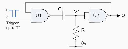
Using NAND gates
Using 555 Timer IC

Bistable Multivibrator

Using BJT

Using NAND gates
Using 555 Timer IC
Astable Multivibrator
Using BJT

Using NAND gates

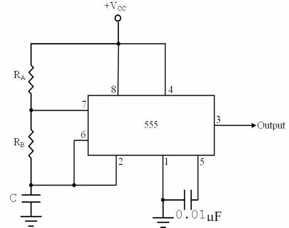
Using 555 Timer IC